Advanced Process Lab Webinar

November 2, 2020

Join us on November 12 for a FREE webinar:

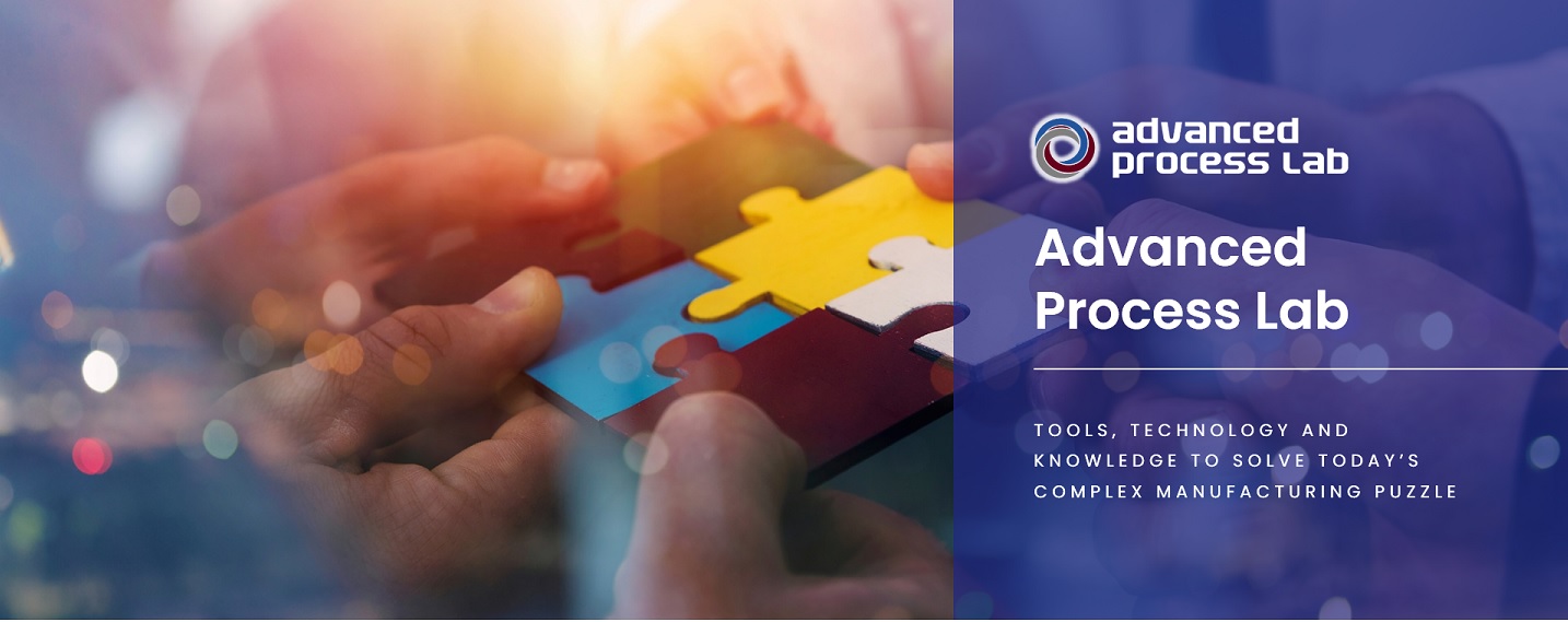
Tools, Tech. & Knowledge to Solve today’s Complex Manufacturing Problems


  • Multiple global time-zone friendly sessions available (@ 9 am,  2 pm & 8:00 pm EDT), click HERE to sign up!

  • Chance to WIN an Amazon or VISA Gift Card; test your trivia knowledge and more. . .

  • Learn about the tips and tricks of how to adapt your processes to fix a bad stencil design


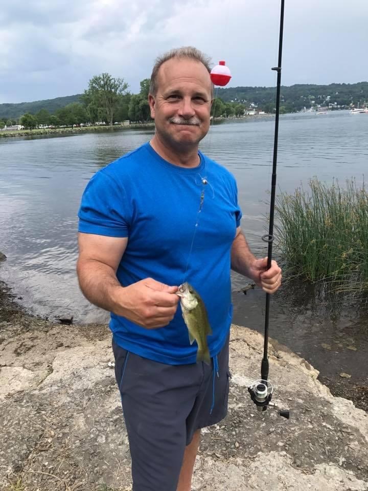
Hosted by Dave Vicari, Director, APL – a scientist (and world-class angler) with 30+ years of broad-based experience in solving the challenges faced by the electronics industry!


At this webinar, you’ll learn about:

  • How the APL can help YOU Build your Best!

  • How to fix a broken product or process


  • Ways to build a new product or build it better and faster

  • How to meet ramp and/or small lot prototype requirements


  • How to access today’s newest manufacturing processes 

  • How the APL brought a product to market and fixed a broken heart


Would you like to build better, faster & smarter or are you interested in learning more about the APL, then sign up below. 

  • Click HERE to sign up for this FREE webinar!


We look forward to seeing you on November 12th.


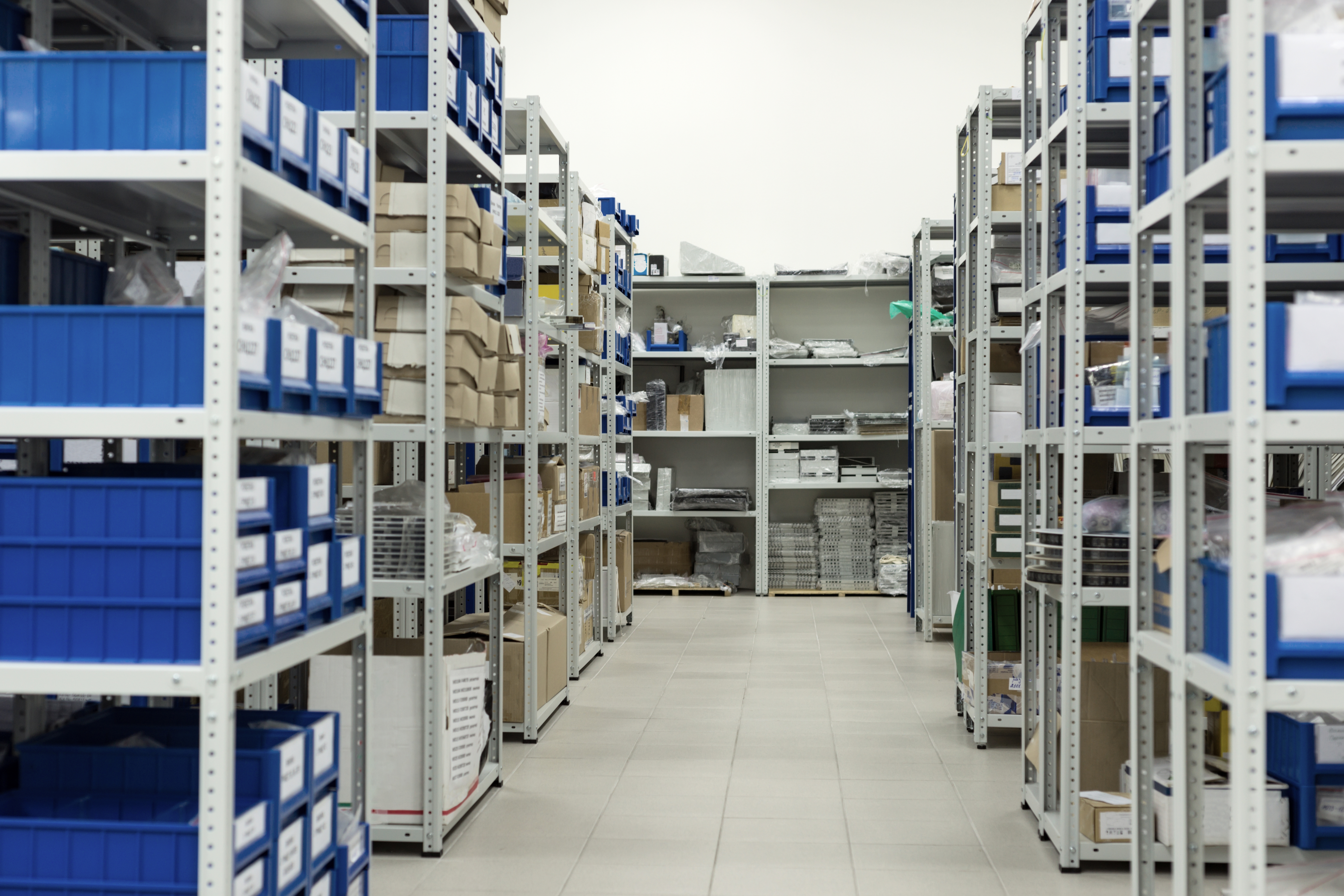
The APL delivers the  knowledge
to help you build better, faster & smarter!

Check out all that the APL has to offer here!


More Related Posts

The Agile Learner: An Ode to e-Learning

In April 2025, I took my first e-Learning course: Surface Mount Operator Suite. I have no formal education in precision automation solutions for the semiconductor and electronics manufacturing industry. With this being said, I was unsure if I’d be able to comprehend the course material, much less keep up with it. After diving in and now completing the course, I can honestly say it is suitable for anyone with the capacity to learn, and it is more user-friendly than I could’ve anticipated.

“Moore” Is Better with Heterogeneous Integration

As Moore’s Law slows, Heterogeneous Integration (H.I.) is emerging as the smarter path forward—combining multiple specialized dies (logic, memory, RF, power) into one compact, high-performance package. This blog explores how H.I. is transforming everything from smartphones to datacenters, and how advanced platforms like FuzionSC™ + High-Speed Wafer Feeder are simplifying complex multi-die assembly. The result? Faster development, lower costs, and better chips—built for the future.

“Fish-Eyed” Press-Fit Pins Challenges & Solutions

Traditional inspection methods fall short when it comes to next-gen “fish-eyed” press-fit pins—whose flared, asymmetrical geometry makes them nearly impossible to evaluate with 2D vision systems. One misaligned pin on a $15K board can mean catastrophic failure down the line. That’s why we’ve implemented precision 3D laser inspection across our platforms—combining upward and downward vision, sub-micron accuracy, and custom tooling to catch defects in real time and ensure flawless placement the first time, every time.