July 6, 2015 – The ESD Association estimates that 25% of all electronics damaged for unknown reasons can be attributed to ESD and the cost of ESD damage to the Electronics Industry to be $5 billion (USD) per year.
What is ESD?
ESD is a build-up of charges over a specific area without current flow. One of its causes is similar or dissimilar material contacting and separating. As long as this build up continues, the charges will increase until they reach a level that breaks down the strength of an insulator (either material or air). The charge or charges will equalize very rapidly, and the equalization is an uncontrolled discharge called an ESD Event. Lightning is an extreme example of an ESD event.
ESD is not a new problem. Black powder manufacturing and other pyrotechnic industries have always been dangerous if an ESD event occurs in the wrong circumstance. During the era of tubes (AKA the good old days of electronics) ESD was a nonexistent issue for electronics, but with the advent of semiconductors and the increase in miniaturization, it has become much more serious.
ESD comes in many forms; it can be as small as 50 volts of electricity being equalized up to tens of thousands of volts. The actual power is extremely small, so small that there is generally no danger to someone who is in the discharge path of ESD. It usually takes several thousand volts for a person to even notice ESD in the form of a spark and the familiar zap that accompanies it. The problem with ESD is that even a small discharge that can go completely unnoticed can ruin semiconductors. A static charge of thousands of volts is common; however it is not a threat because there is no current of any substantial duration behind it. These extreme voltages do allow ionization of the air and allow other materials to break down, which is the root of where the damage comes from.
Damage to components can, and usually does occur when the part is in the ESD path. Many parts, such as power diodes, are very robust and can handle the discharge, but if a part has a small or thin geometry as part of their physical structure then the voltage can break down that part of the semiconductor. Currents during these events become quite high, but are in the nanosecond to microsecond time frame. Part of the component is left permanently damaged by this, which can cause two types of failures; specifically catastrophic and latent damage.
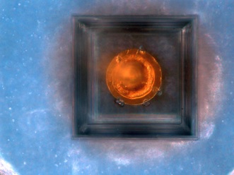
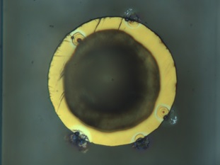
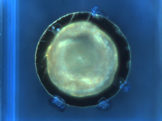
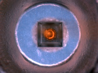
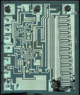
Catastrophic Damage: Once an electronic device is exposed to an ESD event, the device’s circuitry may be permanently damaged causing the device to fail. Usually this can be detected using a basic performance test. The images below of catastrophic ESD damage were provided by Universal Instruments’ Advanced Process Lab who regularly conducts Failure Analysis testing on ESD damaged components. For further information on the APL, visit their website at: https://www.uic.com/solutions/apl
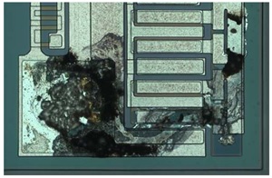
The images below are of a forced 5,000 Watt ESD event performed on an IM LED at Universal’s APL. The pictures are collected from a z-section looking through the lens of the LED directly above the ball bonded die. All four images are of the same sample at different magnifications and illumination techniques. The ESD damage can be detected by looking at the electrical arcing damage surrounding the circumference of the Gold pad on the die surface.
Latent Damage: A device that is exposed to an ESD event may be partially degraded, yet continue to perform its intended function. ESD latent damage may be detectable by its electrical signature but its lifetime behavior is not predictable. *One example can be seen below. Latent damage can result in permanent failure under some stress conditions making the device unreliable.
Latent damage may also allow the problem component to work for hours, days or even months after the initial damage before catastrophic failure. Many times these parts are referred to as the “walking wounded”, since they are working but bad. If these components end up in a life support role, such as medical or military use, then the consequences can be grim.
*Latent damage on a Voltage Regulator, which worked for an hour after the ESD incident.
Ways to prevent ESD Damage:
ESD can be prevented by integrating Electrostatic Discharge Protected Areas (EPAs) into your manufacturing process. The EPA can be a small workstation or a large manufacturing area. The main principle of an EPA is that there are no highly-charged materials in the vicinity of ESD sensitive electronics, all conductive materials are grounded, workers are grounded, and charge build-up on ESD sensitive electronics is prevented. International standards should be used to define a typical EPA and can be found through the International Electro technical Commission (IEC) or American National Standards Institute (ANSI).
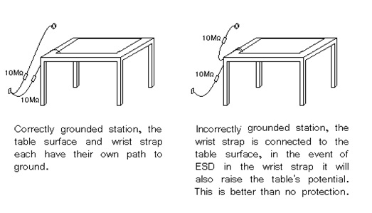
ESD prevention within an EPA may include using appropriate ESD-safe packing material, the use of conductive filaments on garments worn by assembly workers, requirement of *wrist straps and foot-straps to prevent high voltages from accumulating on workers’ bodies, anti-static mats or conductive flooring materials to conduct harmful electric charges away from the work area, and humidity control. Humid conditions prevent electrostatic charge generation because the thin layer of moisture that accumulates on most surfaces serves to dissipate electric charges.
*Example of correctly vs. incorrectly grounded ESD Station
Proper Storage and Transportation of ESD sensitive Component and Boards:
It does no good to take ESD prevention steps if the parts are being damaged while storing or carrying them. The most common method is to use a variation of a *Faraday cage, commonly referred to as an ESD bag.
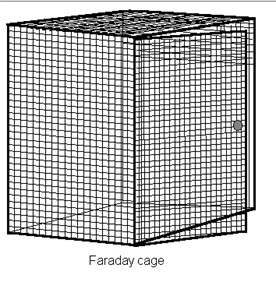
A Faraday cage or Faraday shield is an enclosure formed by conductive material or by a mesh of such material. Such an enclosure blocks external static and non-static electric fields by channeling electricity along and around, but not through, the mesh, providing constant voltage on all sides of the enclosure. Since the difference in voltage is the measure of electrical potential, no current flows through the space.
An ESD bag surrounds the component with a conductive shield, and usually has a non-static generating insulative layer inside. In permanent Faraday cages this shield is grounded, as in the case of RFI (Radio Frequency Interference) rooms, but with portable containers this isn’t practical. By putting an ESD bag on a grounded surface the same thing is accomplished. Faraday cages work by routing the electric charge around the contents and grounding them immediately. A car struck by lightning is an extreme example of a Faraday cage.
Static bags are by far the most common method of storing components and boards. They are made using extremely thin layers of metal, so thin as to be almost transparent. A bag with a hole, even small ones, or one that is not folded on top to seal the content from outside charges is ineffective.
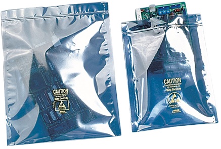
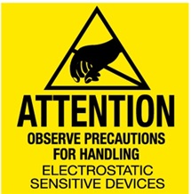
Example of circuit boards being stored in ESD Bags & common Anti-Static Warning Label
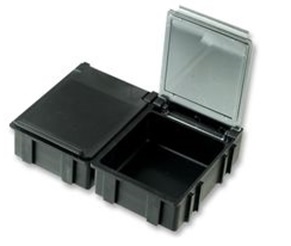
Another method of protecting parts in storage is totes or tubes. In these cases, the parts are put into conductive boxes with a lid of the same material. This effectively forms a Faraday cage. A tube variation – used for IC (Integrated Circuits) and other devices with a lot of pins – stores the parts in a molded conductive plastic tube that keeps the parts safe both mechanically and electrically.
Example of Conductive box
Even components that are considered fairly rugged can be damaged by ESD. Bipolar transistors – the earliest of the solid state amplifiers – are not immune, though less susceptible. Some of the newer high-speed components can be ruined with as little as 3 volts. There are components that might not be considered at risk, such as some specialized resistors and capacitors manufactured using MOS (Metal Oxide Semiconductor) technology, that can be damaged via ESD.
However, there is no such thing as an ESD-Safe machine without an ESD-Safe nozzle and we have talked about this in a previous post “Are Your SMT Machines ESD-Safe?“.
ESD can be a minor unfelt event measuring a few volts, or a massive event presenting real dangers to operators. All ESD protections can be overwhelmed by circumstance, but this can be circumvented by awareness of what ESD is and how to prevent it. Ensuring ESD safety during your manufacturing process is a challenge; however, following the ESD guidelines appropriate for your manufacturing model, properly storing and transporting ESD sensitive boards and components, and purchasing ESD-safe nozzles with ESD-safe properties, will help you to take steps towards eliminating ESD damage and issues with your PCB assembly process!
For questions related to overcoming ESD challenges in the Electronics Industry, contact:
Richard Strube, CMSEÒ
Sr. Product & Safety Code Compliance Engineer
Phone: +1-607-779-5326
E-mail: richard.strube@uic.com
To purchase ESD safe nozzles for your manufacturing process, visit our Tooling Solutions site at: http://parts.uic.com/