Heterogenous Integration Webinar

December 8, 2020

Join us on December 16 for a FREE webinar:

**Place your DIE and Win with Heterogeneous Integration**


  • Multiple global time-zone friendly sessions available (@ 9 am,  2 pm & 8 pm EDT), click HERE to sign up!

  • Chance to WIN an Amazon or VISA Gift Card; test your trivia knowledge and more. . .

  • Take a spin on the APAS Acronym Slots to learn the meaning behind a few common APAS terms


Learn  more about the exciting Advanced Packaging technology
Heterogeneous Integration (HI)

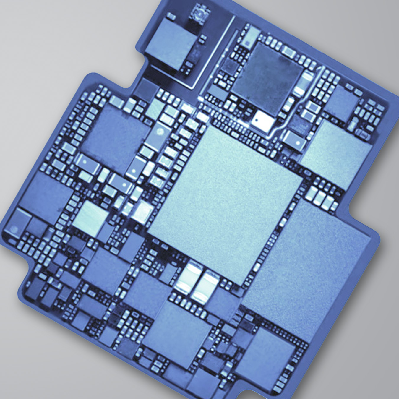
Example of a SiP module which requires HI for cost-effective assembly.

  • HI refers to the integration of multiple component types (die, MEMS, passive, etc.) into a higher-level assembly (or system-in-package), which delivers increased functionality at a lower cost.

  • HI presents a distinctive set of challenges which require unique assembly solutions.  What are those challenges and what are the potential solutions for cost-effective multi-die assembly?

  • What markets will benefit from HI and how will it enable the world’s most innovative products for 5G, AI, Edge Computing and more. . .

  • Click HERE to sign up!


Hosted by Glenn Farris, VP Strategic Marketinga industry expert with 30+ years of broad-based experience implementing solutions to address the challenges faced by the Advanced Packaging industry.  

Glenn Farris, VP Strategic Marketing


At this webinar, you’ll learn about:

  • What’s the big deal with Heterogeneous Integration (HI) and what benefits does it provide?

  • What are the markets and outlook for HI?

  • Why is HI essential for today’s leading-edge technologies?

  • What are the challenges and assembly solutions for HI?

  • Click HERE to sign up!


We look forward to seeing you on December 16!

More Related Posts

The Agile Learner: An Ode to e-Learning

In April 2025, I took my first e-Learning course: Surface Mount Operator Suite. I have no formal education in precision automation solutions for the semiconductor and electronics manufacturing industry. With this being said, I was unsure if I’d be able to comprehend the course material, much less keep up with it. After diving in and now completing the course, I can honestly say it is suitable for anyone with the capacity to learn, and it is more user-friendly than I could’ve anticipated.

“Moore” Is Better with Heterogeneous Integration

As Moore’s Law slows, Heterogeneous Integration (H.I.) is emerging as the smarter path forward—combining multiple specialized dies (logic, memory, RF, power) into one compact, high-performance package. This blog explores how H.I. is transforming everything from smartphones to datacenters, and how advanced platforms like FuzionSC™ + High-Speed Wafer Feeder are simplifying complex multi-die assembly. The result? Faster development, lower costs, and better chips—built for the future.

“Fish-Eyed” Press-Fit Pins Challenges & Solutions

Traditional inspection methods fall short when it comes to next-gen “fish-eyed” press-fit pins—whose flared, asymmetrical geometry makes them nearly impossible to evaluate with 2D vision systems. One misaligned pin on a $15K board can mean catastrophic failure down the line. That’s why we’ve implemented precision 3D laser inspection across our platforms—combining upward and downward vision, sub-micron accuracy, and custom tooling to catch defects in real time and ensure flawless placement the first time, every time.