Smarter, Faster, Cheaper: A New Way to Build Tomorrow’s Electronics
Every year, our devices — phones, laptops, wearables — get faster, thinner, and cheaper. But behind the scenes, maintaining that pace is getting tougher.
We surfed the wave of Moore’s Law for decades — doubling transistor counts every couple of years to boost performance and drop costs. But that curve is flattening. Designing the latest chips at advanced nodes now costs up to 8x more than a decade ago.
So, how do we keep the innovation engine running – enter Heterogeneous Integration (H.I.)!
One Package, Many Talents: The Genius of Heterogeneous Integration
At the heart of H.I. is a deceptively simple but incredibly powerful idea: instead of one big chip doing everything, why not build a system where each chip — or die — does what it does best?
An H.I. circuit is like the tech world’s version of a dream team. On a typical H.I. device, you have:
- 3 to 4 different types of dies — each with a specific job.
- 1 to 8 of each kind of die, which depends on performance, redundancy, or memory needs.
Each of these die types performs a different function:
- A CPU or GPU die runs the core computations.
- A high-speed memory die feeds data at lightning speed.
- An RF die handles wireless communication.
- A power management die keeps the whole thing running cool and efficiently.
All of this lives inside one tightly integrated package — like packing a laptop’s worth of computing muscle into something the size of your fingernail.
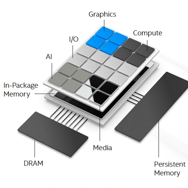
Example of Heterogeneous Integration packaging.
And the beauty of it? These dies can come from different fabrication nodes, wafer sizes, and foundries. You’re no longer stuck with a single monolithic design or tied to one manufacturing process. That means faster development cycles, better performance optimization, and lower costs.
With H.I., you can mix and match the best technologies — logic from one provider, memory from another, sensors from a third — making custom silicon at scale not just possible, but practical.
Where does H.I.Technology show up?
Semiconductor chips are ubiquitous; they power the electronics you use every day. These chips are at the heart of:
- Smartphones, where space is limited but performance demands are sky-high.
- Wearables need to be ultra-thin, power-efficient, and packed with sensors.
- Datacenter accelerators, where high-bandwidth memory and logic must coexist.
- Satellites and aerospace systems, where reliability and compactness are everything.
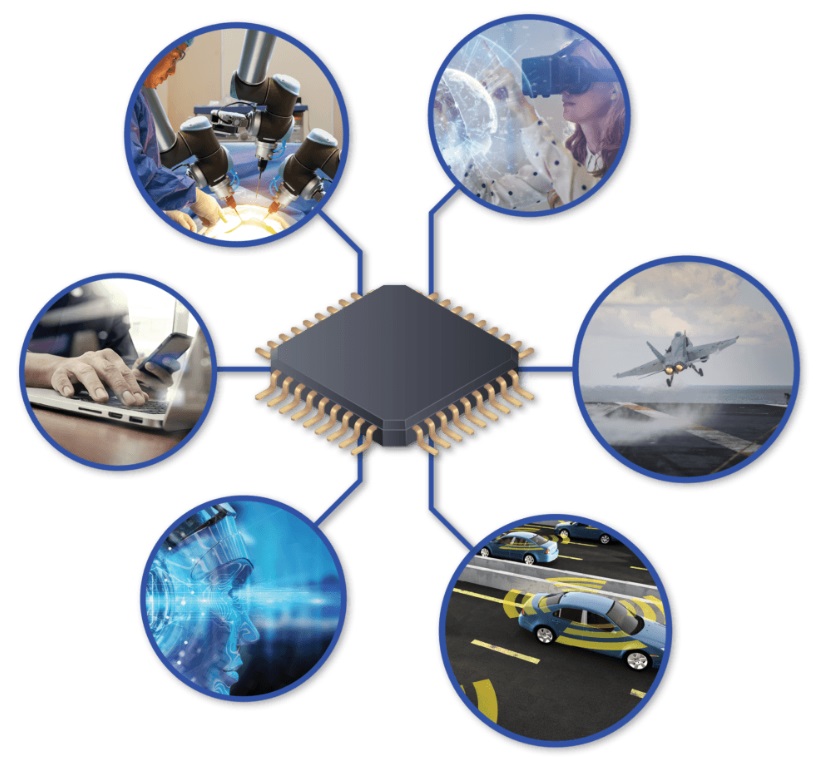
Semiconductors are the brains behind all of our modern devices.
Heterogeneous Integration Assembly Considerations
In H.I., getting the right chips in the right place is only half the battle. Just as a race car needs the right chassis for its engine, H.I. needs the right substrate — the physical and electrical foundation that holds everything together. With dies of varying sizes, functions, and sources, substrates must be versatile, robust, and precise. Let’s break it down: die presentation and substrate type.
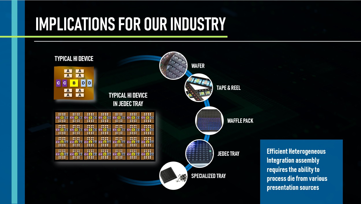
Die Presentation Methods
Before a single die is placed, it has to be delivered to the assembly system in a format that supports high-mix, high-precision processing. How the die is presented can make or break efficiency. Here are a few standard formats:
- Wafer on Tape Frame: The most common format for H.I.—ideal for high-volume, automated placement of known good dies (KGDs).
- Fan-Out Wafer or Panel: This is essential for fan-out H.I., where dies are redistributed onto a carrier for high-density integration.
- JEDEC Tray: Typically used for packaged dies or legacy formats.
- Gel-Pak: Best for fragile or unique die types, especially in low-volume or prototype H.I.
- Waffle Pack: This is a solid choice for low—to mid-volume H.I. or when dies are too thick or thin for standard automation.

Various die presentation formats
What Are the Best Substrates?
Once the dies are presented, they need a landing zone that supports power delivery, signal integrity, thermal management, and mechanical reliability — all while enabling compact, modular designs. Here are a few of the substrate types and where they shine:
- Silicon Interposers: High-speed, fine-pitch routing for 2.5D integration.
- Fan-Out Substrates (RDL): Spreads I/O over a larger area.
- Organic Substrates: Cost-effective PCB option for modular designs.
More Die Types = More Problems:
Now that you’ve seen how dies are laid out in their various presentation formats and what substrates they go on, the next big question is: how do you actually assemble a H.I. device?
Here’s the thing—more dies (or more part numbers) means more manufacturing headaches.
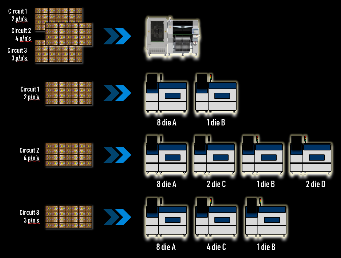
Traditionally, H.I. assembly has meant using a multi-system setup, where each die and wafer type needs its own dedicated equipment. So if you’re building a package with four different die types, each in varying quantities and wafer formats, you might end up needing three separate lines and nine machines just to assemble a single device. That’s a lot of complexity to manage, not to mention the floor space, labor, and overhead it eats up.
Let’s break it down. In a multi-system setup for three circuits, you’d need three separate lines configured like this:
-
Circuit 1: 8 Die A, 8 Die B
-
Circuit 2: 8 Die A, 2 Die C, 1 Die B, 2 Die D
-
Circuit 3: 8 Die A, 4 Die C, 1 Die D
Now compare that to a single-system setup, where all die—regardless of type— and wafer format, are placed on a shared line. One line, all parts, no juggling machines.
Single System vs. Multiple Dedicated System Line
What are the economic detractors of this type of setup?
-
Lower yield: More part handling and more chances for vision errors
-
Lower throughput: Unbalanced lines mean idle machines
-
Higher operating costs: More operators and more floor space
-
Low OEE: Idle capacity from line-device mismatch
It’s like trying to make a sandwich with every ingredient coming from a different kitchen—or to put it another way: too many cooks, no chef. The result? Slow, expensive, and error-prone.
A Smarter Way: One Single-System for ALL:
That’s where a single-system approach shines. You consolidate all die types onto one line, handled by a unified system. It simplifies the process, boosts scalability, and helps you keep up as H.I. designs grow in complexity. Think of it like a master chef crafting your sandwich from start to finish—no handoffs, no delays. Clean. Fast. Consistent.
So, why choose a single system that handles all of the multi-die placement considerations? Here are just a few reasons:
🧩 Pre-sequences 4 part types — No juggling
🔀 Places 4 die types in one cell — No reconfiguring of lines
👤 Runs with just 1 operator — Less labor
🎛️ One setup for any Heterogeneous Integration device — Simplifies the complex
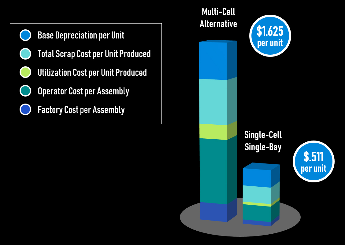
Economic benefits of Single-Cell system vs. Multi-Cell Alternative
📊 Curious about the math behind this? The *paper this blog is based on breaks it down—and spoiler alert: the single-system approach wins in every single category. [Read the paper here: https://www.uic.com/wp-content/uploads/2025/05/Assembly-Solutions-for-Cost-Effective-HI_Paper_Final.pdf]
*Thanks to Glenn Farris, our former VP of Marketing, whose original paper inspired this post.
The Game-Changer: A Single-System Powerhouse
Say hello to the future of H.I. The FuzionSC Semiconductor Platform + High-Speed Wafer Feeder (HSWF) is built for speed, precision, and high-mix scalability — the ultimate multi-die single-system placement solution.
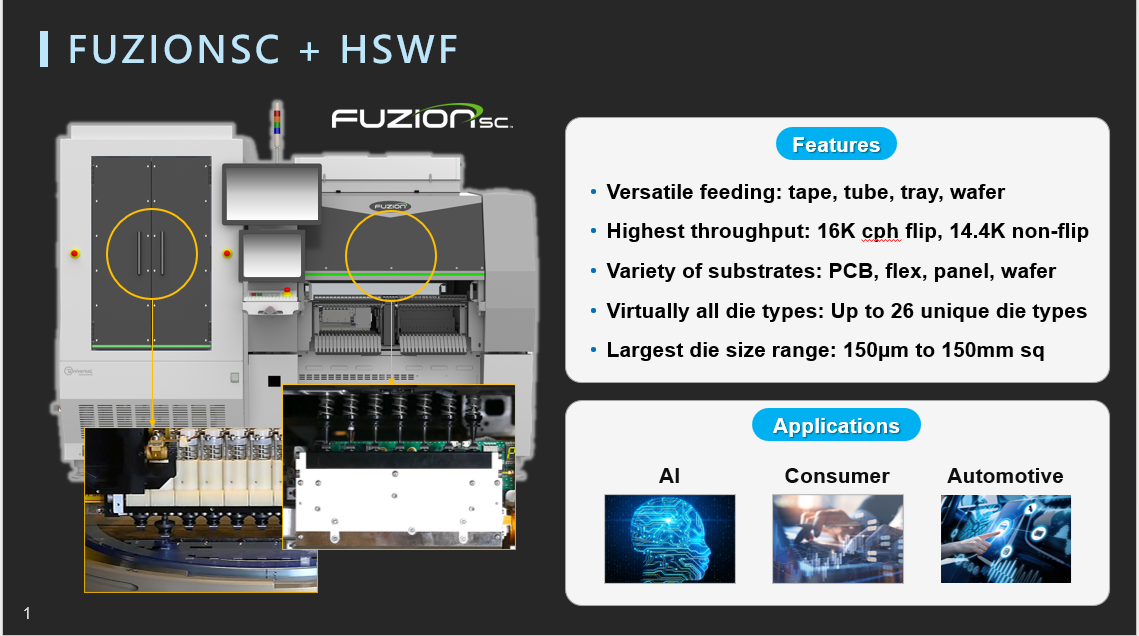
High-Speed, Flexible Die Handling — Ready for Anything
-
Direct Die Picking: Works with wafers, tape, or trays — no extra prep needed.
-
Easy Wafer Handling: Pre-stretched wafers and multi-wafer carousels simplify die release and enable quick changeovers.
-
Broad Compatibility: Supports wafer sizes from 100 mm to 300 mm and handles up to 26 part numbers in one run.
-
Precision Placement: Accurately places dies as thin as 50 microns with sub-micron precision.
-
High Throughput: Up to 16,000 placements per hour with 14 precision pick heads and real-time alignment.
-
Versatile Assembly: Places both active and passive components on one platform.
See the system in action here:
Learn more here: https://www.uic.com/products-advanced-packaging/
From 2.5D to 3D, fan-out to high-mix —FuzionSC + HSWF is engineered to make complex H.I. simpler, faster, and more cost-effective.
The Bottom Line: Build Smarter, not Harder!
Heterogeneous Integration is the future — but the old-school, one-system-per-die method isn’t built for it.
Smarter tools like FuzionSC + HSWF make building faster, smaller, and more affordable devices at scale possible and practical.
In short: Smarter assembly = better chips = better tech for everyone. Now, that’s a better way to “Moore”.