August 1, 2014 – It has been more than 5 years when the first generation of Package-on-Package came into form. The primary objective is to combine the memory and the application specific integrated circuit (ASIC) to use much lesser real property this shrinking the overall package. However, it is known fact that even with this 3D assembly technology, the demand for continuous higher functionality and smaller form factor is ever present.
In discussing about the continuing shrinking form factor, active and passive components are becoming part of the substrate thus further reducing the height of the package. All of these are going to be discusses and presented here including the most economical advanced packaging assembly technique.
Mobile Computing Trends
- Mobile is becoming the single device that does everything
- Requires high computing performance at low power
- High performance is a small form factor: Fine pitch/smaller bumps; Higher density/fine spacing
- Pace of shrinking lithography is slowing down, driving verticality (2.5D & 3D): New challenges for manufacturers: new materials, complex processes, multiple processes on a single platform; Thinner die and substrate
Why Package-on-Package
- Drives miniaturization (smaller & lighter)
- Better electrical performance at lower power
- Memory can be tested separately form logic
- Only “know good” packages are used
- End user controls logistics (logic decoupled from memory)
- Any mechanically mating memory can be used
- Logic suppliers don’t need to “deal” with the memory
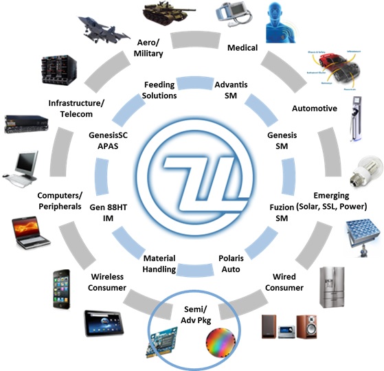
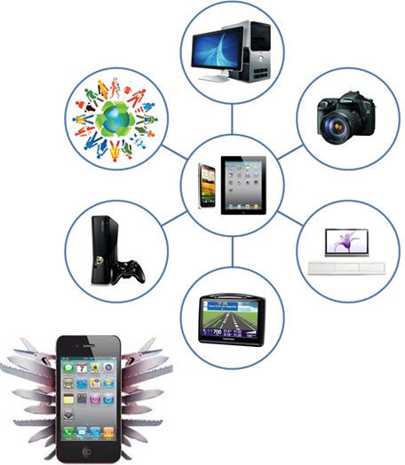
- Major applications: Wireless technologies (mobile phones, tablets, GPS, PDAs); Digital cameras; Broadband; Gaming and other mobile applications
Processor-Memory Stacking Solution
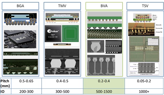
BVA offers the advantages of TSV (fine pitch and high number of interconnects) while utilizing existing packaging materials, processes and infrastructure.
BVA PoP: Wide IO Support without TSV
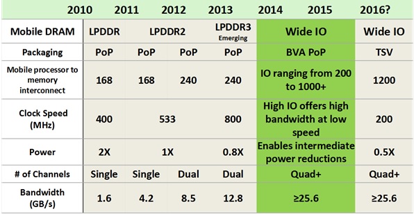
- Wide IO is an order of Magnitude increase in IO compared to current memory interface
- Wide IO implementation with TSV is not expected in the next few years
- Bond Via Array (BVA) is an attempt at offering wide IO using current PoP infrastructure
Bond Via Array (BVA) Package
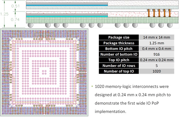
1020 memory-logic interconnects were designed at 0.24mm*0.24mm pitch to demonstrate the first wide IO PoP implementation.
PoP Package Parameters
- Ball pitch (logic & memory) – 240um to 650um
- Ball alloy – 104, 305, 405, (SAC or Tin/Silver) Tin/Lead, etc
- Ball size – generally a function of pitch (175um up to 390um)
- Bump & wire (BVA) planarity
- Bump & wire (BVA) solderability
- Package moisture up take: JEDEC Level 1-6 (tested at level 3): How long can part be exposed before bake is needed?
PoP Package Warpage
1st Generation PoP (Standard BGA and CSP format)
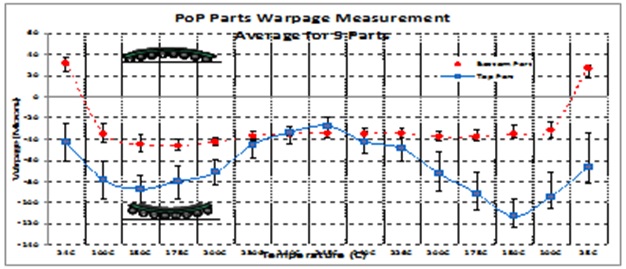
- Overall magnitude < 90um
- Matching not the best but somewhat typical
- JEIDA standard 7306: At 0.5mm pitch; Max warpage 110 microns
2nd Generation PoP – TMV (Through Mold Via)
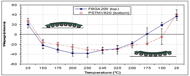
- Overall magnitude < 50um
- Excellent matching
- JEIDA standard 7306: At 0.5mm pitch; Max warpage 110 microns
Next Generation PoP
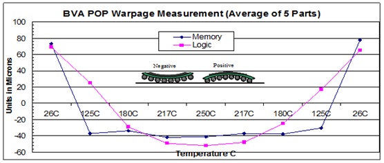
- Overall magnitude < 100um
- Excellent matching
BVA Process Optimazation
Assembly Process Steps, Reliability & Quality Analysis:
- PCB design & parameters
- Screen printing process parameters
- Stencil design & parameters
- Screen printing results
- Flux application
- Assembly = Stack on PCB (end product) & pre-stack
- Mass reflow parameters
- Reliability enhancement
- Reliability testing
- Assembly quality analysis
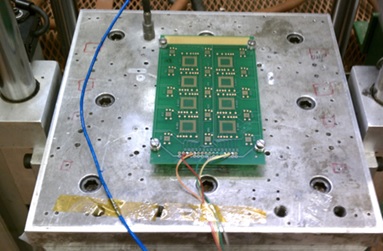
Note: The optimization was conducted in Advanced Process Laboratory of Universal Instruments.
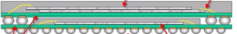
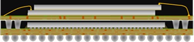
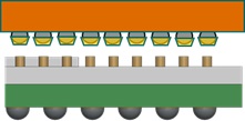
Left: Illustration of PCB pad for PoP
Middle: Illustration of BVA PoP – Cross Sectioned
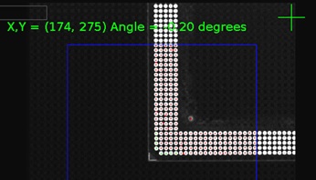
Right: Illustration of vision inspection of bottom PoP
PCB Design and Parameters
900 I/O to route (14mm*14mm)
- Solder Mask (SMD) or Non-solder Mark Defined Pads (NSMD): SMD if preferred for attachment pad size consistency. NSMD is better for pad cratering, etc.
- Via in pad or top side traces (dog bone with via), if via in pad is used the via should be filled & level with the pad
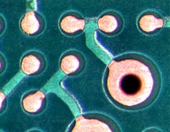
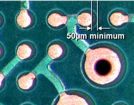
- Pad size should be approximately 50% to 57% of the pitch
- Solder mask should be a minimum of 50um for overlap (SMD) or cut back for NSMD
- Attachment Pad Finish: Ni/Gold; OSP Copper; Immersion Tin; Immersion Silver
- Fiducials: If SMD pads are used, SMD fiducials should be designed in the application at the local placement site(s)
Left: SMD
Right: NSMD
Screen Printing Process Parameters
- Major Printing Process Parameters: Squeegee material: Electro-form, stainless, etc; Squeegee angle: 60 degree preferred; Squeegee pressure: Variable dependent; Print velocity: Aperture size & solder paste rheology dependent (through put); Separation velocity; Print gap: On or off content; PCB support (tooling)
- Print Process Control for Small Apertures:Control time between prints – drying time & underside “bleed” out
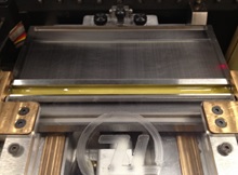
- “Newer” Screen Printer Technology: Ultra Sonic squeegee
Left: Ultra Sonic Squeegee
Right: 0.3mm pitch PoP
Stencil Design and Parameters
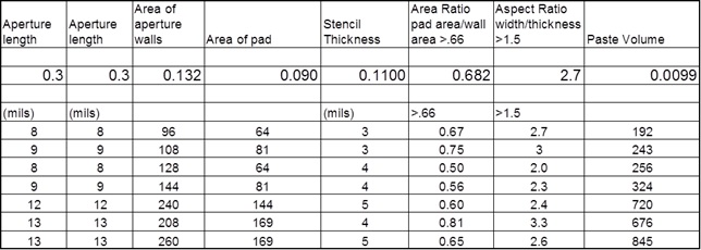
- PoP Stencil Design: Stencil thickness: Pitch & application component mix driven (75um to 125um range for most applications); Aperture shape = Rounded corner squares recommended; Aperture size = Pitch & warpage driven (adjustment based on warpage), approximately 64% of pitch; Area ration – Excel file that automatically calculates area ratio (greater than 0.66 recommended)
- Stencil Technology: Laser cut; Electro-form; Nano coating
Stencil Parameters Table
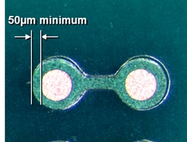
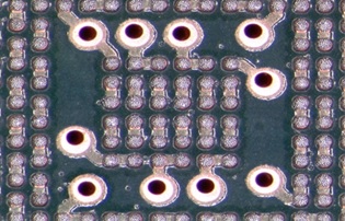
Screen Printing Results 0.4mm Pitch
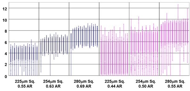
- 15 Prints per test condition, no under stencil cleans between strokes
- Each scatterplot group represents all print deposits on the board (15 components/9300 paste deposits
- DEK Galaxy Printer, foil-less clamps, vacuum tooling pins, 60 degrees metal squeegee, V=30mm/s, P=4.6kg, Separation=20mm/sec
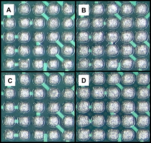
A: 127um stencil, 254um apertures, oo much variability, lowest area ration
B: 127um stencil, 280um aperture, bridging risk
C: 101.6um stencil, 254um apertures, robust process
D: 101.6um stencil, 280um apertures, bridging risk
Flux Application
- Major Flux Variables:Viscosity & rheology; Tack; Flux type (no clean, water soluble); Post reflow solids percentage; Halogen free; Compatibility with other materials: printed solder paste, underfill, etc.
- Linear Thin Film Applicator (flux application): Linear actuation for thickness uniformity; Broad viscosity range supported (under 200 to over 900 centipoise); Gang or individual dip processing; Quick release tooling for easy cleaning; Cavity plate assures accurate material thickness repeatability; Dipping based on Force; Dip verification based on spindle impact sensing
Left: Illustration of flux distribution on LTFA
Middle: Structure of LTFA
Right: Illustration of fluxed PoP
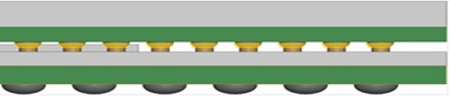
BVA PoP Assembly
- Two types of PoP assembly: Stack on printed circuit board (end product); Pre-stacked on spindle impact sensing
Left: Stacked on PCB (end product)
Right: Pre-stacked
Assembly Process Flow
- Screen print solder paste (standard process)
- Placement process:Transfer PCB into top surface justify clamp PCB assembly; Perform Global/local PCB fuducial inspection; Pick-up logic, inspect 7 solder bumps in each of 4 corners (28 balls total) & place at 100 to 150 grams; Vision inspect BVA pins (9-16 pins in each of 4 corners, 36 to 64 pins total); Pick-up memory, vision inspection one corner (9 bumps) for part present to ensure memory is present before dipping; Die memory into tacky flux (0.115um film thickness, 127um plate); Inspect 9 solder bumps in each of 4 corners (36 balls total) & place at 30 grams; Mass reflow (standard process)
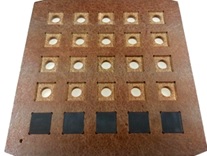
Left: Logic Balls (bottom side)
Middle: Logic Pins (top side)
Right: Memory Balls (bottom side)
High-Performance Package Assembly
- GenesisSC Platform: all-in-one platform: Silicon/SMT, high accuracy/high-speed assembly; High accuracy: (±10um,
Pre-Stack Assembly Process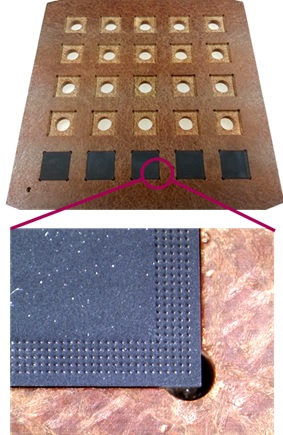
- Pallet design
- Protection of logic solder balls during assembly (don’t want to flat spot solder balls)
- Pallet material – Durastone, etc (ESD & machinable)
- Pad/pin site find should be used for alignment (just before each placement)
- Provides for manufacturing flexibly & one LTFA to supply multiple assembly lines
- Down side – Extra reflow cycle, storage for moisture up take has to be addressed (desiccant & vacuum seal or bake out)
- New tray need for “stacked” package (trays from logic & memory will not work)
- Pre-stack process is fully automated start to finish
Major Mass Reflow Parameters
- Air or Nitrogen environment
- Single ramp or two-step profile
- Flux activation time
- Peak temperature
- Time above liquids (void reduction)
- Optimizing profile for two different flux systems?
- Most PoP package have fairly low thermal mass
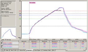
Reflow Profile and Cross-Section after Reflow
Reliability Enhancement
- Application reliability: No post assembly reliability enhancement; Underfill (logic & memory); Edge bond; Dam & fill
- Flux residue & underfill compatibility
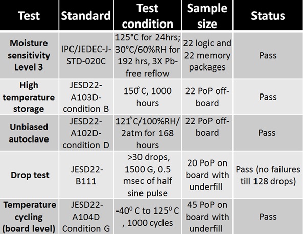
Reliability Testing
- Thermal cycle and/or shock
- Bend
- Drop
- Vibration
- Unbiased autoclave
- High temperature storage
- Liquid to liquid
- Moisture sensitivity level

Shock Response Test
Reliability Testing Results
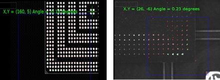
Assembly Quality Analysis
- X-ray (2D & 3D)
- Visual (outer rows)
- Acoustic microscope C-SAM (underfill)
- Cross-section and/or flat sections
- Dye penetration
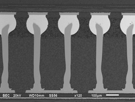
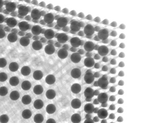
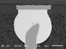
Left: Cross-Section Illustration
Right: X-ray Results
The demand for thinner and smaller form factor device with high capacity memory and high I/O application IC will be increasing. The tablet, smartphone and other mobile gadgets are the primary users of this type of devices. These devices are expected to grow more and more. As this requirement is already happening in our midst, the assembly solution, process and materials should be ready to meet it and a feasible solution is now available.