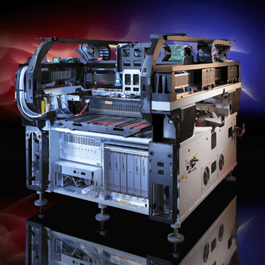
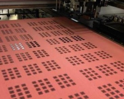
December 3, 2014 – Semiconductor packaging has traditionally followed dedicated equipment sets for given package formats or processes dictated by Bare Die or Flip Chip assembly. New Package Functionality, Performance, Miniaturization, Low cost materials are driving the ever import Time to Market product life. As these challenges are common place in the industry it is ultimately important to drive lower assembly costs through the morphing of new and traditional packaging on a larger scale enabling the processing of more packages per single process operation. Packing technique such as eWLB/FO WLP, Embedded, SiP, RCP and 2D/3D assembly are targeting benefits of large scale assembly for KGD and post process cost benefits. The demands of 4um to 10um die placement accuracy are now open to processes and assembly techniques on a Scale exceeding 600mm x 600mm panel formats previously restricted to < 300mm x 300mm.
Theoretical Aspects
Today’s High Accuracy assembly of Flip Chip correlates to assembly rates <5k cph and Lower Accuracy less complex assembly of Die at assembly rates >8k cph. The association of Speed and Accuracy are typically on opposing ends however the nature to the link is not often revealed or available in the same system. High Accuracy placement machines cannot go faster and a High Speed machine cannot simply be more accurate by going slower as it is not the intent of the design architecture.
Imagine exploiting capability from the assembly needs from both Semiconductor and SMT assembly. Targeting value added performance enhancers to enable new placement equipment to operate in modes of High Accuracy of Semiconductor assembly but at speeds competitive to SMT High Speed rates. It all starts with the design architecture or foundation, starting from the leveling pad to the spindle/manipulator used to handle the device.
Architecture Enabling Large Area Assembly
Principle of construction
A robust construction consisting of a rigid base to manage vibration and isolation of neighboring vibrations is a must. Linear Motor driven axis offer a clean propulsion system with fast motion response and settling times essential to speed and accuracy. Traditional permanent magnet linear motors are susceptible to high temperature excursions in high duty cycle operation; Variable Reluctance Linear Motors operate much cooler and are preferred. Linear motors also offer no restriction to length of construction enabling to simply grow the motor stator to match the construction size. Multiple heads spindles/manipulators reduce the number of cycles between pick and place allowing axis speed to be less critical to overall assembly rates.
All together the construction sets the foundation for large area assembly without compromise to speed and accuracy.
Techniques to enable high accuracy placement
Importance to Mapping
Because of mechanical non-uniformities, each positioning system behaves uniquely. This causes any absolute vector from encoder position to a particular location to differ from the predicted location, making it impossible to perform absolute moves and realize large area assembly. In other words, having the axis move ½ meter in any direction from encoder (0,0) may result in a final destination of slightly less than ½ meter while on another machine construction the final destination may be slightly more than ½ meter. To resolve this problem, a machine map must be generated to describe the behavior of the positioning system imperfections matching encoder locations to machine locations.
Enhanced Mapping
Mapping models the behavior of the positioning system and relates encoder coordinate locations to machine coordinates.
Machine locations are typically defined by the mapping plate(s), and encoder locations are defined by the (X,Y) linear encoders located on the X and Y beams. Plate size and grid size establishes the area and mapping resolution. Enhanced mapping is a process in which additional steps are taken to model the grid points through certified measurements allowing the use of actual grid positions over nominal for a refined resolution.
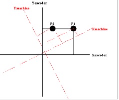
Note that in the encoder coordinate system, moving from P1 to P2 is purely an X movement. However, when the same movement is done in the machine coordinate system, both an X and a Y movement are required. Because of these spatial differences, both an X and a Y map are generated to translate between the two coordinate systems.
Techniques to Accuracy Stability
AOI feedback
Often placement systems accuracy performance metrics are either self-verified or validated through capable automated optical inspection AOI systems. The challenge between these processes is that as they may agree on repeatability they often do not agree on means. Therefore a method to align to an established reference or benchmark is important to the system use and verification of duplicate systems.
Techniques to administer AOI feedback into the placement system with the goal to refine each placement or spindle bias to a nominal placement coordinate are essential. Nominal by placement bias techniques enables the proficiency of multi spindle systems for higher throughputs without accuracy deficiencies. The uses of these corrections are also beneficial to post process steps which may require up stream corrections to accommodate or enhance performance conditions of final process. ie. Mold operations or thermal effects on materials. Software utilities enable the seamless import of offset data into the placement system. High material counts and HVM can only be realized by leveraging the abilities of process feedback from the AOI systems.
Stability
Dynamic Placement Calibration Verification
System stability is essential to high accuracy placement throughout changes in ambient temperature or operational duty cycles.
In addition to aforementioned techniques and construction one unique method is to self-monitor change through self-calibration techniques or dynamic placement calibration verification (DPCV). DPCV employs the use of verified reference artifacts to enable self-measurable change in placement performance in both repeatability and bias from an established reference. The sub-micron measurement technique eliminates contribution of positioning system from the measurement error and is therefore able to detect true system change. Its operation is automatic without operator intervention and may be set to perform based on conditions of change in time, product or temperature changes. The use of this feature maintains system performance stability, SPC and is ideal for planned maintenance indicators.
High Accuracy through Top Align Process TAP
Semiconductor assembly in which the active face up typically relegates to low accuracy assembly. The statement is in part due to in nature of traditional assembly techniques and the fact that the die active surface cannot be imaged while being help by the pick tip or spindle/manipulator. These barriers are now eliminated through TAP. TAP is a process in which the die outline saw cut and active pattern are inspected simultaneously by an (downward) inspection camera. The inspection establishes a relationship between the die outline versus the die patterns. Following Top inspection the die is picked as it is performed traditionally and moved to an upward looking camera. The upward camera defines the relationship of the die outline to the spindle for placement. The relationship offset from the TAP process is added to the upward camera correction offset for final placement. This process resolves the issue of component movement between inspect and pick.
CONCLUSION
Assembly of Semiconductor and SMT share the same requirements of High Speed and High Accuracy however they carry different numbers of reality. Semiconductor assembly has parallel requirements for pick and place solutions and now has the ability to realize complete system flexibility, small strips to large panel sizes as well as <10um placement accuracy. Thus enabling the ability to offer lower cost packaging for FOWLP, Embedded, SiP, RCP and Die Stacking.
For more information about Universal Instruments’ solutions on Advanced Packaging/Semiconductor Packaging, please visit https://www.uic.com/solutions/advanced-packaging/.